

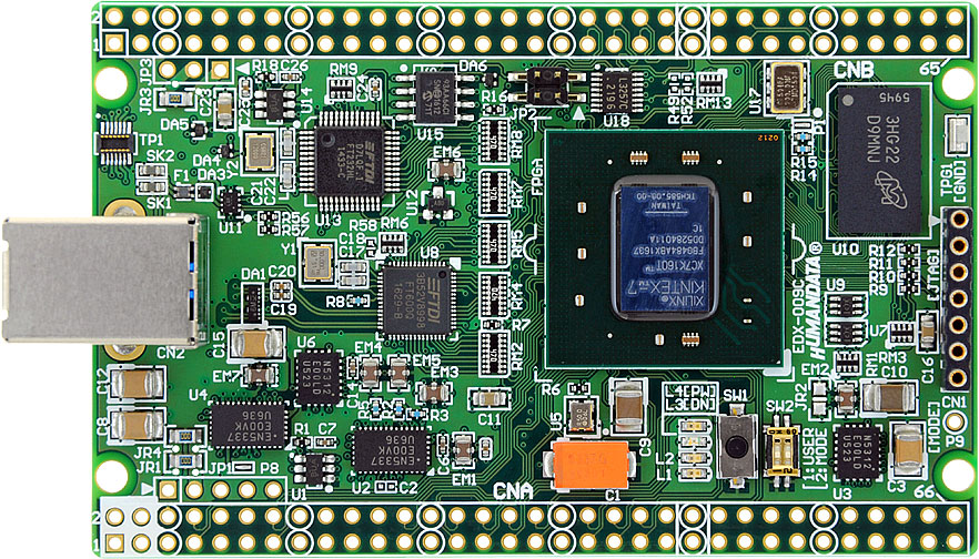
Kintex-7 USB-FPGA board with FTDI USB3.0 bridge IC

Overview
EDX-009 is AMD Hi-performance Kintex-7 USB-FPGA board. EDX-009 is compact and very simple. EDX-009 operates with single 5.0V power supply. An FTDI's FT600 offers USB3.0 bridge to FPGA user communication I/F. An FT232H is mounted for FPGA configuration.
No download cable is needed to configure the FPGA with HuMANDATA original configuration tool "BBC[EDX-009]".
Rev4: The production of the Power IC (Enpirion) on the board was discontinued. So the part has been changed to the alternative and the board was revised.
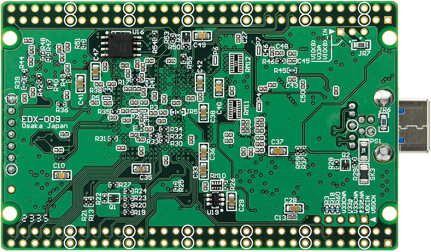
For more details, please refer to the circuit schematics.
» Please also see other FT600 series products.
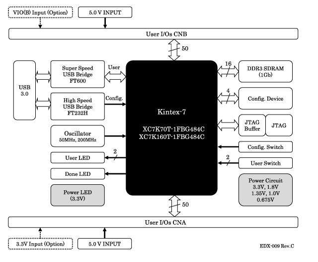
Block Diagram
Specifications
- FPGA: AMD Kintex-7
- XC7K70T-1FBG484C
- XC7K160T-1FBG484CFeature XC7K70T XC7K160T Logic Cell 65,600 162,240 Slice 10,250 25,350 Max Distributed RAM (kb) 838 2,188 Max Block RAM (kb) 4,860 11,700 DSP Slice 240 600 CMT (MMCMx1+PLLx1) 6 8 Maximum user I/O pins(Device) 300 400 Maximum user I/O pins(Board) 100 100 This table is for reference. Please refer to official data-sheets for certain information.
- Power: 5.0V or 3.3V single power supply operation
- Controlled power on sequence - 100 I/O PAD 100 mil (2.54 mm) grid
- DDR3 SDRAM: MT41K64M16 (Micron, 1Gbit)
High density is available by a BTO up to 4Gbit - Configuration Device
Rev3: Quad SPI ROM: MT25QL128 (Micron, 128Mbit)
Rev1, 2: Quad SPI ROM: N25Q128 (Micron, 128Mbit) - USB3.0 bridge IC (FTDI, FT600)
- User communication I/F - USB2.0 bridge IC (FTDI, FT232H)
- User communication I/F
- FPGA Configuration
- Configuration device access (Write/Reset/Erase)
- Free Original Configuration Tool " BBC[EDX-009]" - ESD protection for USB2.0 I/F
- On-board Oscillator: 50MHz, 200MHz (LVDS)
- External clock inputs are available (CNA/CNB) - User Switch x2 (Push x1, Slide x1)
- User LED x2
- Status LED x2 (Power, Done)
- Power-on Reset
- JTAG Connector(7 pin socket) for download cable connection
- JTAG buffer for stable download and debug - High quality 8 layers PCB (Immersion gold)
- Credit-Card-Size 3.386"x 2.126" (86 x 54 mm)
- Tested all I/O
- RoHS compliance
- MADE IN JAPAN
Reference Data
- USB SuperSpeed connection check by a USB 3.0 test tool
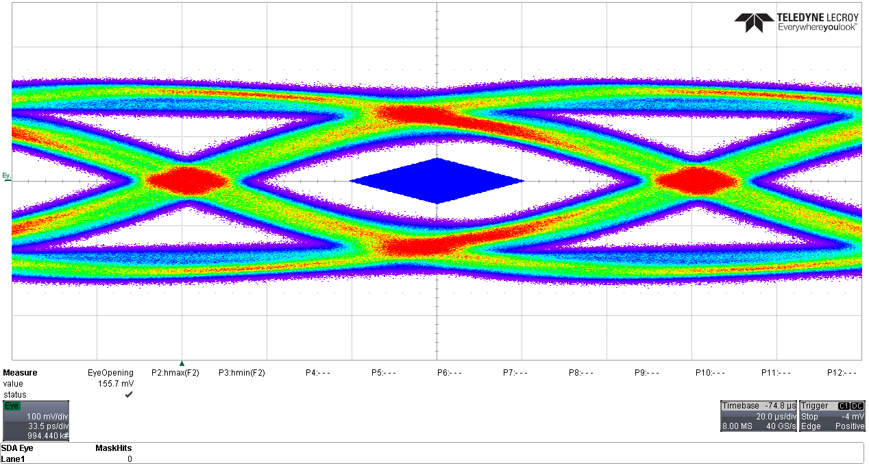
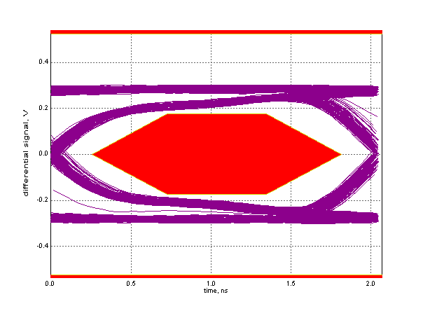
- USB HighSpeed Compliance Test. Eye pattern of upstream tests. (FT600)
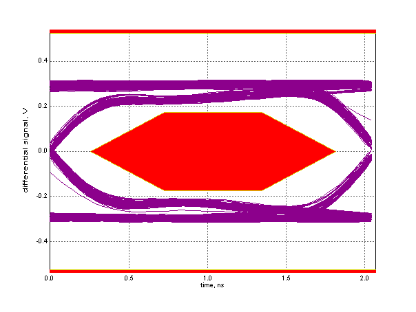
- USB HighSpeed Compliance Test. Eye pattern of upstream tests. (FT232H)
Package Contents
| Item | Image | Quantity |
|---|---|---|
| USB-FPGA board (EDX-009) |  |
1 |
| USB3.0 cable (Type A to B) | 1 | |
| Pin Headers |  |
2 |
| Sockets |  |
2 |
There is no paper document such as user's manual and circuit schematic in the package.
Please download those documents from the link in the documentation section below.
Documentation
Price and Add-ons
| Description | Model (order code) |
FPGA | List price |
Stock Status |
|---|---|---|---|---|
| USB 3.0 with Kintex-7 USB-FPGA board | EDX-009-70T | XC7K70T-1FBG484C | ||
| USB 3.0 with Kintex-7 USB-FPGA board | EDX-009-160T | XC7K160T-1FBG484C | ||
| Universal board with 3.3V10A DC/DC POWER SUPPLY |
ZKB-054 | - | ||
| Universal board for ACM/XCM-0 series (Type2) | ZKB-105 | - |
[ ]