

Kintex-7 FBG676 FPGA board

Overview
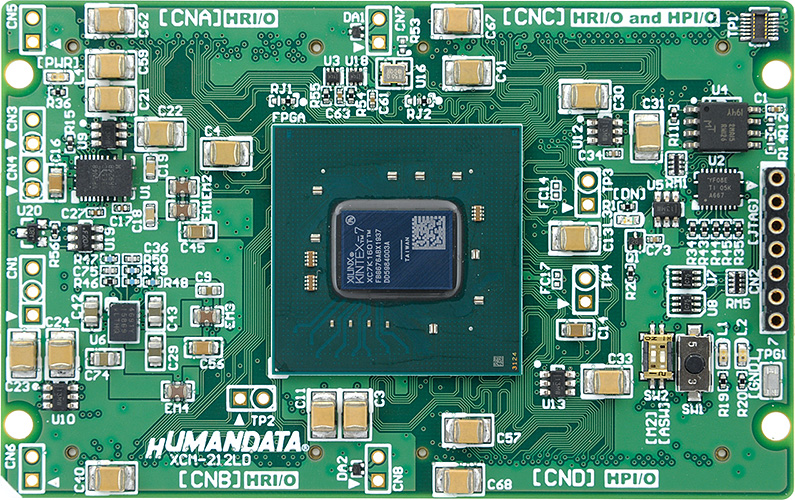
AMD Kintex-7 FBG676 High Performance FPGA Board. XCM-212L has voltage regulators, an oscillator, user LEDs, switches and a configuration device on its compact credit-card size board.
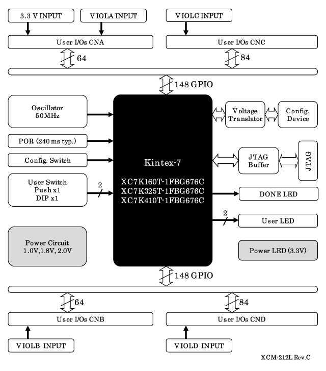
There are 296 user I/Os divided into four Vcco groups.
Rev2: The production of the Power IC (Enpirion) on the board was discontinued. So the part has been changed to the alternative and the board was revised.
For more details, please refer to the circuit schematics.
Block Diagram
Specifications
- FPGA: Kintex-7
- XC7K160T-1FBG676C
- XC7K325T-1FBG676C
- XC7K410T-1FBG676CFeature XC7K160T XC7K325T XC7K410T Logic Cells 162,240 326,080 406,720 Slice 25,350 50,950 63,550 Maximum Distributed RAM (kb) 2,188 4,000 5,663 Total Block RAM (kb) 11,700 16,020 28,620 DSP Slices 600 840 1,540 CMT (MMCMx1+PLLx1) 8 10 10 Max user I/O (Device) 400 500 500 Max user I/O (Board) 296
(HR 172)
(HP 124)296
(HR 172)
(HP 124)296
(HR 172)
(HP 124)This table is for reference. Please refer to official data-sheets for certain information.
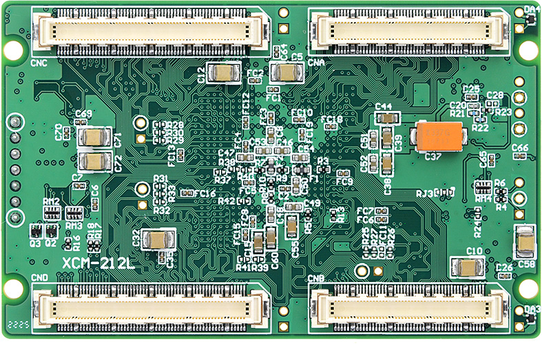
- User I/O: 296 (HIROSE connectors, 80 pin x2, 100 pin x2)
- IOA (CNA Connector): 64 (HR)
- IOB (CNB Connector): 64 (HR)
- IOC (CNC Connector): 84 (HR 44, HP 40)
- IOD (CND Connector): 84 (HP)
* External power is needed for I/O (VCCOA/VCCOB/VCCOC/VCCOD)
* HR = High-range I/O with support for I/O voltage from 1.2V to 3.3V.
* HP = High-performance I/O with support for I/O voltage from 1.2V to 1.8V. - Power: 3.3V, VIOLA, VIOLB, VIOLC, VIOLD
- VCCINT, 1.0/1.8/2.0V are generated by on-board regulators
- Sequenced power supplies (Power on) - Separable VCCO (CNA/CNB/CNC/CND)
- Configuration Device:
Quad SPI ROM: MT25QL128 (Micron, 128Mbit) - 50 MHz Oscillator (50 ppm) or External inputs
- Power-on Reset IC for FPGA configuration
- User Switch x 2 (Push x1, DIP x1bit)
- User LED x 2
- Status LED x2 (Power, Done)
- JTAG port (7 pin socket)
- JTAG buffer for stable download and debug
- Configuration device
- High quality eight layer PCB (Immersion gold)
- Credit-Card-Size 3.386"x 2.126" (86 x 54 mm)
- Tested all I/Os
- RoHS compliance
- MADE IN JAPAN
Package Contents
| Item | Image | Quantity |
|---|---|---|
| FPGA Board (XCM-212L-***) |  |
1 |
| Sockets (HIROSE 80P) | 2 | |
| Sockets (HIROSE 100P) | 2 |
There is no paper document such as user's manual and circuit schematic in the package.
Please download those documents from the link in the documentation section below.
Documentation
Price and Add-ons
| Description | Model (order code) |
FPGA | List price |
Stock Status |
|---|---|---|---|---|
| Kintex-7 FBG676 FPGA board | XCM-212L-160T | XC7K160T-1FBG676C | ||
| Kintex-7 FBG676 FPGA board | XCM-212L-325T | XC7K325T-1FBG676C | ||
| Kintex-7 FBG676 FPGA board | XCM-212L-410T | XC7K410T-1FBG676C | ||
| Universal board for ACM/XCM-1L, 2L series (MAX 1.8 V) | ZKB-157L | - |
[ ]
 EDA-013 is Intel Corp.'s High performance USB-FPGA Cyclone 10 LP board.