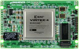
Xilinx Virtex-4 FFG1148 FPGA board
*This series was discontinued.
Overview
Xilinx Virtex-4 FFG1148 pin High Performance FPGA Board. XCM-202 is simple and easy to use. It's Compact size. 3.3V single power supply operation.
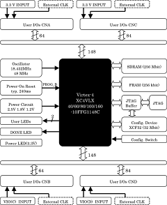
Block Diagram
Contents
- Xilinx XC4VLX40-10FFG1148C or
Xilinx XC4VLX60-10FFG1148CFeature XC4VLX40 XC4VLX60 Slices 18,432 26,624 Logic Cells 41,472 59,904 Maximum Distributed RAM Bits 288 416 Maximum user I/O pins(Device) 640 640 Maximum user I/O pins(Board) 296 296 Maximum Differential I/O Pairs 320 320 Total Block RAM Bits 1,728 K 2,880 K DCMs 8 8 DSP48As 64 64 This table is for reference. Please refer to official data-sheets for certain information.
- Configuration Device (Xilinx XCF32PVOG48C)
- 296 I/O two HIROSE connectors and two 100 pin HIROSE connectors
(exist dedicate input pin for external CLOCK inputs) - Separable VCCO
- 48MHz / 18.432MHz Oscillator (50 ppm) or External
- SDRAM 256 M (16 M x 16) (Micron MT48LC16M16A2P-75-D)
- FRAM 256 kbit (32k x 8) (RAMTRON FM18L08)
- 8 test points for debug
- Power-on Reset IC
- JTAG port (7 pin Header)
- JTAG buffer for stable download or debug
- 3.3 V single power supply operation with on-board 1.2 V / 1.8 V / 2.5 V regulators
- High quality ten layers PCB. (Immersion gold)
- Credit-Card-Size 3.386" x 2.126" (86 x 54 mm)
- Tested all I/O
- Non-use of 6 Restricted substances of RoHS directive
- MADE IN JAPAN
Package Contents
| Item | Image | Quantity |
|---|---|---|
| FPGA board (XCM-202-***) |  |
1 |
| Sockets (HIROSE 80pin) |  |
2 |
| Sockets (HIROSE 100pin) |  |
2 |
There is no paper document such as user's manual and circuit schematic in the package.
Please download those documents from the link in the documentation section below.
Documentation
Price and Add-ons
| Description | Model (order code) |
FPGA | List price |
Stock Status |
|---|---|---|---|---|
| Virtex-4 FFG1148 FPGA board | XCM-202-LX40 | XC4VLX40-10FFG1148C | ||
| Virtex-4 FFG1148 FPGA board | XCM-202-LX60 | XC4VLX60-10FFG1148C | ||
| Pitch Conversion Board ACM/XCM-2 series | ZKB-041KIT | - |
[]


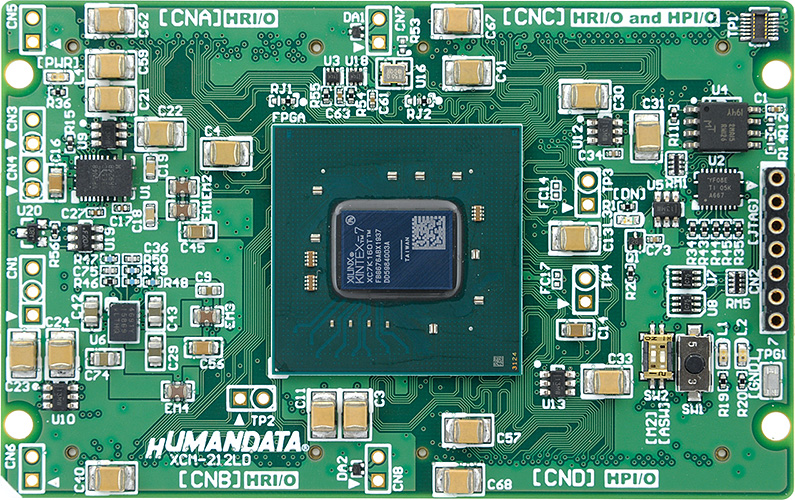
 XCM-212L is an evaluation board equipped with a XILINX's high performance FPGA, Kintex-7 ( FBG676 package).
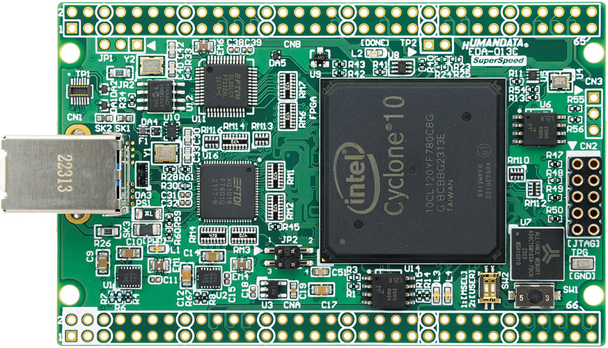
 EDA-013 is Intel Corp.'s High performance USB-FPGA Cyclone 10 LP board.