Altera MAX 10 F672 FPGA board
Overview
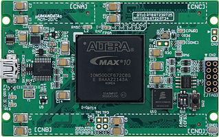
ACM-207 is Altera Hi-performance FPGA MAX 10 board. It's compact and very simple. 3.3V single power supply operation.
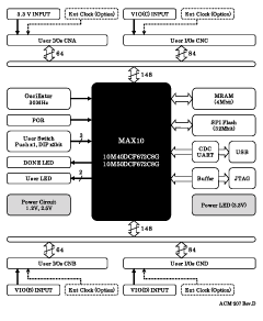
Block Diagram
Specifications
- FPGA: Altera MAX 10
- 10M40DCF672C8G
- 10M50DCF672C8GFeature 10M40 10M50 Logic Elements 40 K 50 K Memory: M9K (kb) 1,260 1,260 PLLs 4 4 Maximum user I/O pins(Device) 500 500 Maximum user I/O pins(Board) 296 296 User Flash Memory (kb) 5,888 5,888 18 x 18 Multipliers 4 4 This table is for reference. Please refer to official data-sheets for certain information.
- Power : 3.3 V single supply
- 2.5 V and 1.2 V on-board regulators - MRAM: MR2A16AMA35 (256Kx16bit)
- Internal Configuration Device
- SPI-FLASH ROM: N25Q032 (Micron, 32Mbit)
- USB-UART I/F
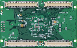
- User I/O : 296 (HIROSE connectors, 80 pin x2, 100 pin x2)
- Separable VCCIO
- Tested all I/O - Oscillator : 30 MHz
- External clock input pins - User Switch x3
- Push x1
- DIP x2 bit - User LED x2
- Status LED (Power, Done)
- Power-on Reset IC
- JTAG Connector (10 pin socket) for download cable connection
- JTAG buffer for stable download and debug - High quality eight layer PCB.(Immersion gold)
- Credit-Card-Size 3.386" x 2.126" (86 x 54 mm)
- RoHS compliance
- MADE IN JAPAN
Package Contents
| Item | Image | Quantity |
|---|---|---|
| FPGA Board (ACM-207-***) |  |
1 |
| Sockets (HIROSE 80P) | 2 | |
| Sockets (HIROSE 100P) | 2 |
There is no paper document such as user's manual and circuit schematic in the package.
Please download those documents from the link in the documentation section below.
Documentation
Price and Add-ons
| Description | Model (order code) |
FPGA | List price |
Stock Status |
|---|---|---|---|---|
| MAX 10 F672 FPGA board | ACM-207-40 | 10M40DCF672C8G | ||
| MAX 10 F672 FPGA board | ACM-207-50 | 10M50DCF672C8G | ||
| Universal board for ACM/XCM-1, 2 series (MAX 3.3 V) | ZKB-157 | - | ||
| Pitch Conversion Board ACM/XCM-2 series | ZKB-041KIT | - |



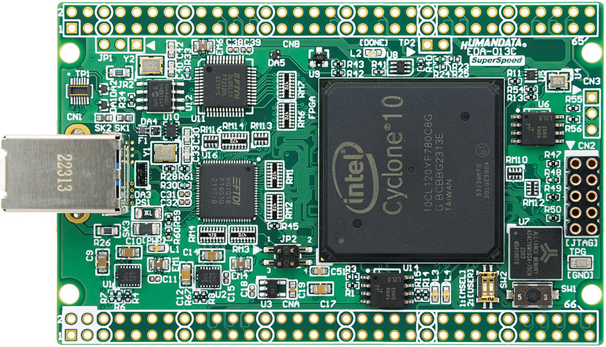 EDA-013 is Intel Corp.'s High performance USB-FPGA Cyclone 10 LP board.
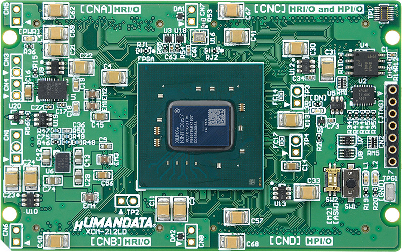 XCM-212L is an evaluation board equipped with a XILINX's high performance FPGA, Kintex-7 ( FBG676 package).