

Artix UltraScale+ FFVB676 FPGA board

Overview
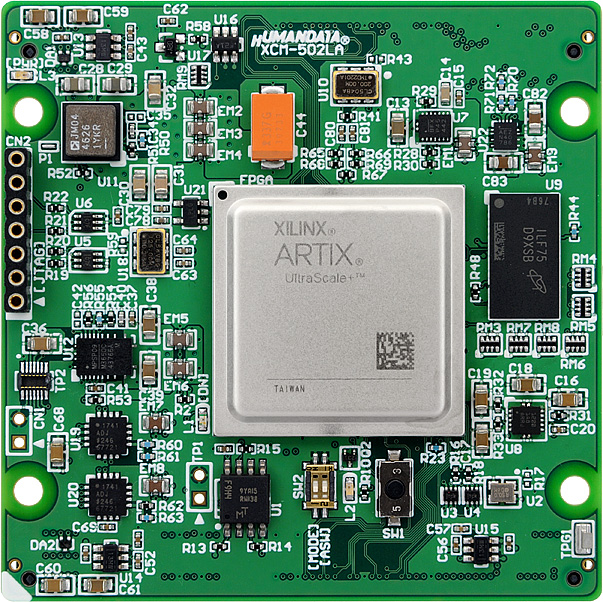
AMD Artix UltraScale+ FFVB676 High Performance FPGA Board. XCM-502L has voltage regulators, an oscillator, user LEDs, switches and a configuration device on its compact size board.
There are 128 user I/Os divided into two Vcco groups.
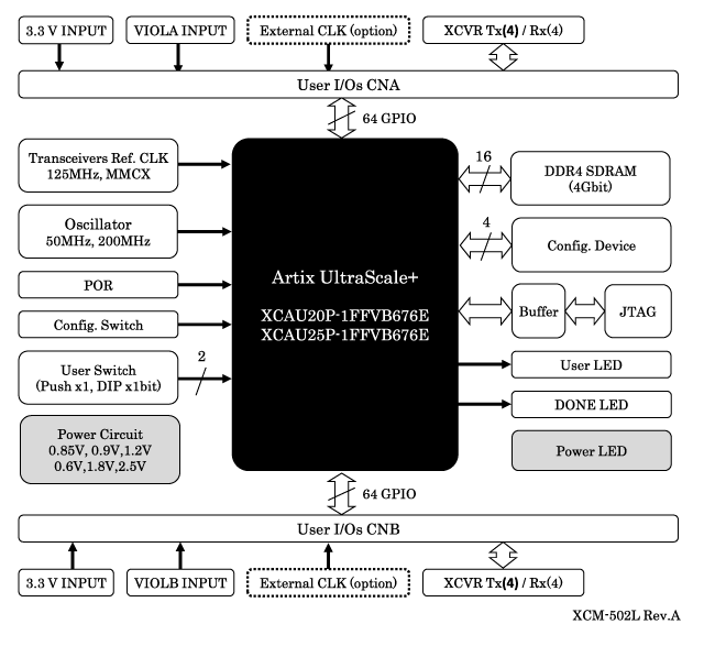
Block Diagram
Typical Eye Diagram
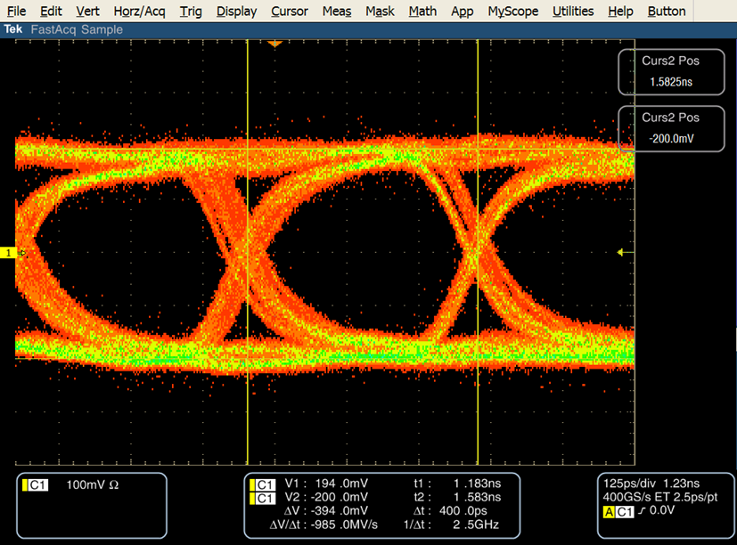 Click to Zoom |
Channel: 225_X0Y0(P) Ref.Clk: 125MHz Rate: 2.5Gbps Swing:950mVppd (1100) Pre/Post-cursor: 0 dB Data: PRBS-7 Trigger: Rising Edge Signal Path: ZKB-155L |
Specifications
- Artix UltraScale+
- XCAU20P-1FFVB676E
- XCAU25P-1FFVB676E
Feature XCAU20P XCAU25P System Logic Cells 238,437 308,437 CLB Flip-Flops 218,000 282,000 CLB LUTs 109,000 141,000 Maximum Distributed RAM (Mb) 3.2 4.7 Block RAM Blocks 200 300 Block RAM (Mb) 7.0 10.5 UltraRAM Blocks - - UltraRAM (Mb) - - CMTs (1MMCM and 2PLLs) 3 4 DSP Slices 900 1,200 System Monitor 1 1 Max HD I/O (Device) 72 96 Max HD I/O (Board) 64 64 Max HP I/O (Device) 156 208 Max HP I/O (Board) 64 64 This table is for reference. Please refer to official data-sheets for certain information.
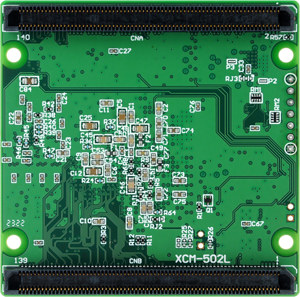
- User I/O: 128 (samtec connectors, 140 pin x2)
CNA: 64 (HD), CNB: 64 (HP)
* External power is needed for I/O (VCCOA/VCCOB)
* HD = High Density I/O with support for I/O voltage from 1.2V to 3.3V.
* HP = High-performance I/O with support for I/O voltage from 1.0V to 1.8V. - Power: 3.3V, VCCOA, VCCOB
- VCCINT, 0.85V, 0.9V, 1.2V, 1.8V, 2.5V, 0.6V on-board regulators
- Sequenced power supplies (Power on) - Separable VCCO (CNA/CNB)
- GTX Transceivers
- Reference clocks: 125 MHz (LVDS)
- Pair of Tx/Rx is led out to each connector
CNA: TX/RX 4ch
CNB: TX/RX 4ch
- Reference clock can be input from CNA/CNB connector - High speed connector of samtec ERF8/ERM8 is adopted
- DDR4 SDRAM
MT40A256M16LY-062E:F (Micron, 4Gbit) - Configuration Device:
Quad SPI ROM: MT25QU128 (Micron, 128Mbit) - on board clocks
- 50 MHz, 200 MHz (LVDS) or External inputs - Power-on Reset IC for FPGA configuration
- User Switch x 2 (Push x1, DIP x1bit)
- User LED x 1
- Status LED x2 (Power, Done)
- JTAG port (7 pin socket)
- JTAG buffer for stable download and debug
- High quality ten layer PCB (Immersion gold)
- Size: 2.559"x 2.559" (65 x 65 mm)
- Tested all I/Os
- RoHS compliance
- MADE IN JAPAN
Package Contents
| Item | Image | Quantity |
|---|---|---|
| FPGA Board (XCM-502L-***) | 1 | |
| Sockets (samtec 140P) | 2 |
There is no paper document such as user's manual and circuit schematic in the package.
Please download those documents from the link in the documentation section below.
Documentation
Price and Add-ons
| Description | Model (order code) |
FPGA | List price |
Stock Status |
|---|---|---|---|---|
| Artix UltraScale+ FFVB676 FPGA board | XCM-502L-20P | XCAU20P-1FFVB676E | ||
| Artix UltraScale+ FFVB676 FPGA board | XCM-502L-25P | XCAU25P-1FFVB676E | ||
| Universal board for ACM/XCM-5L series (MAX1.8V) | ZKB-155L | - |