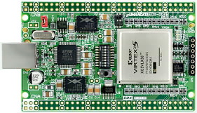
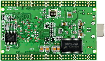
Xilinx Virtex-5 USB-FPGA board
*This series was discontinued.
Overview
EDX-006 is Xilinx's Hi-performance FPGA Virtex-5 board. It's compact and very simple. 5.0 V single external power supply operation.
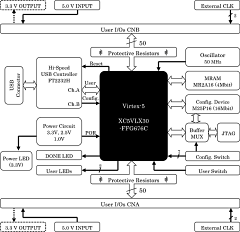
Block Diagram
Specifications
-
XILINX XC5VLX30-1FFG676C
Feature XC5VLX30-1FFG676C System Gates 7,200 Logic Cells 30,720 Maximum Distributed RAM bits 480 K Maximum user I/O pins(Device) 440 Maximum user I/O pins(Board) 100 Total Block RAM bits 1,728 K DCMs 12 PLLs 6 DSP48As 48 This table is for reference. Please refer to official data-sheets for certain information.
- Configuration Device(ST, M25P16-VMF)
- USB Configuration(Download cable is not required)
- Resister-protected 100 I/O, PAD 100 mil (2.54 mm) grid
- FPGA configuration through JTAG
- FPGA configuration through USB
-
User communication through USB
(FT2232H Sync-FIFO mode is available.) - 50 MHz Oscillator(50 ppm)or External
- One User Push-Button Switch
- Two User LEDs
- Two Status LEDs(Power, Done)
- MRAM(EVERSPIN, MR2A16AYS35 256Kx16)
- Power-on Reset
- JTAG Connector(7 pin socket)
- JTAG buffer for stable download or debug
- 5.0 V single power supply operation with on-board 1.0 V/2.5 V/3.3 V regulators
- High quality six layers PCB.(Immersion gold)
- Credit-Card-Size 3.386" x 2.126" (86 x 54 mm)
- ESD and Surge protection for USB
- Tested all I/O
- Non-use of 6 Restricted substances of RoHS directive
- MADE IN JAPAN
Package Contents
| Item | Image | Quantity |
|---|---|---|
| FPGA board(EDX-006) |
 |
1 |
| USB cable(Type A to B) | 1 | |
| Pin Headers |
 |
2 |
| Sockets |
 |
2 |
There is no paper document such as user's manual and circuit schematic in the package.
Please download those documents from the link in the documentation section below.
Documentation
Price and Add-ons
| Description |
Model (order code) |
FPGA |
List price |
Stock Status |
|---|---|---|---|---|
| Virtex-5 USB-FPGA board | EDX-006 | XC5VLX30-1FFG676C | ||
|
Universal board with 3.3V10A DC/DC POWER SUPPLY |
ZKB-054 | - |
[]


