

Kintex-7 FPGA board

Overview
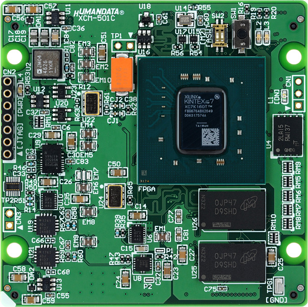
AMD Kintex-7 FBG676 High Performance FPGA Board. XCM-501 has voltage regulators, an oscillator, user LEDs, switches and a configuration device on its compact size board.
There are 128 user I/Os divided into two Vcco groups.
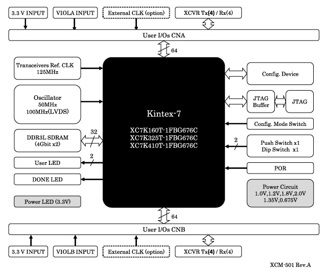
Block Diagram
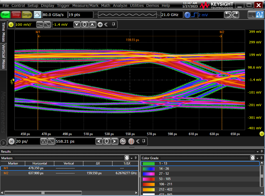
Typical Eye Diagram
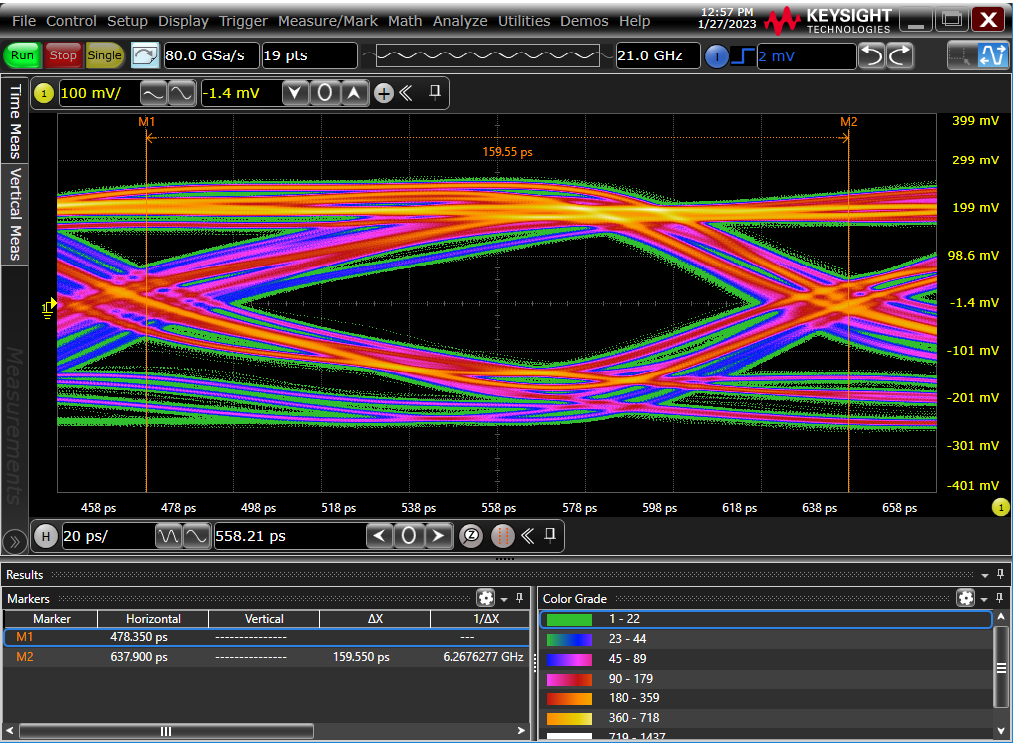 Click to Zoom |
Channel: MGT_TXAP0 Ref.Clk: 125MHz Rate: 6.25Gbps Data: PRBS-7 Trigger: Rising Edge Device:XC7K160T-1FBG676 Signal Path: ZKB-155 |
 Click to Zoom |
Channel: MGT_TXBP0 Ref.Clk: 125MHz Rate: 6.25Gbps Data: PRBS-7 Trigger: Rising Edge Device:XC7K160T-1FBG676 Signal Path: ZKB-155 |
Specifications
- Kintex Kintex-7
- XC7K160T-1FBG676C
- XC7K325T-1FBG676C
- XC7K410T-1FBG676CFeature XC7K160T XC7K325T XC7K410T Logic Cells 162,240 326,080 406,720 Slice 25,350 50,950 63,550 Maximum Distributed RAM (kb) 2,188 4,000 5,663 Total Block RAM (kb) 11,700 16,020 28,620 DSP Slices 600 840 1,540 CMT (MMCMx1+PLLx1) 8 10 10 GTX Channel (Device) 4 8 8 GTX Channel (Board) 4 8 8 Max user I/O (Device) 400 500 500 Max user I/O (Board) 128 128 128 This table is for reference. Please refer to official data-sheets for certain information.
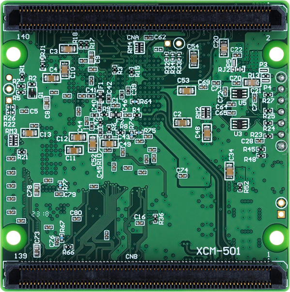
- User I/O : 128 (samtec connectors, 140 pin x2)
* External power is needed for I/O (VCCOA/VCCOB) - Power : 3.3V,
- 1.0V, 1.2V, 1.35V, 0.675V, 1.8V, 2.0V on-board regulators
- Power for I/O (VIOLA/VIOLB) is needed to be supplied from CNA and CNB
- Sequenced power supplies (Power on) - Separable VCCO (CNA/CNB)
- GTX Transceivers
- Reference clocks: 125 MHz (LVDS)
- Pair of Tx/Rx is led out to each connector
CNA: TX/RX 4ch
CNB: TX/RX 4ch
- Reference clock can be input from CNA/CNB connector - High speed connector of samtec ERF8/ERM8 is adopted
- DDR3L SDRAM
MT41K256M16 (Micron, 4 Gbit) x 2 (=32bit wide) - Configuration Device:
Quad SPI ROM: MT25QL128 (Micron, 128Mbit) - on board clocks
- 50 MHz, 100 MHz (LVDS) or External inputs - Power-on Reset IC for FPGA configuration
- User Switch x 2 (Push x1, DIP x1bit)
- User LED x 2
- Status LED x2 (Power, Done)
- JTAG port (7 pin socket)
- JTAG buffer for stable download and debug
- Configuration device
- High quality eight layer PCB (Immersion gold)
- Size: 2.559"x 2.559" (65 x 65 mm)
- Tested all I/Os
- RoHS compliance
- MADE IN JAPAN
Package Contents
| Item | Image | Quantity |
|---|---|---|
| FPGA Board (XCM-501-***) | 1 | |
| Sockets (samtec 140P) | 2 |
There is no paper document such as user's manual and circuit schematic in the package.
Please download those documents from the link in the documentation section below.
Documentation
Price and Add-ons
| Description | Model (order code) |
FPGA | List price |
Stock Status |
|---|---|---|---|---|
| Kintex-7 FPGA board | XCM-501-160T | XC7K160T-1FBG676C | ||
| Kintex-7 FPGA board | XCM-501-325T | XC7K325T-1FBG676C | ||
| Kintex-7 FPGA board | XCM-501-410T | XC7K410T-1FBG676C | ||
| Universal board for ACM/XCM-5 series (MAX3.3V) | ZKB-155 | - |
